Balbharti Maharashtra State Board 11th Physics Textbook Solutions
Chapter 14 Semiconductors Textbook Exercise Questions and Answers.
1. Choose the correct option.
Question 1.
Electric conduction through a semiconductor is due to:
(A) Electrons
(B) holes
(C) none of these
(D) both electrons and holes
Answer:
(D) both electrons and holes

Question 2.
The energy levels of holes are:
(A) in the valence band
(B) in the conduction band
(C) in the band gap but close to valence band
(D) in the band gap but close to conduction band
Answer:
(C) in the band gap but close to valence band
Question 3.
Current through a reverse biased p-n junction, increases abruptly at:
(A) Breakdown voltage
(B) 0.0 V
(C) 0.3V
(D) 0.7V
Answer:
(A) Breakdown voltage
Question 4.
A reverse biased diode, is equivalent to:
(A) an off switch
(B) an on switch
(C) a low resistance
(D) none of the above
Answer:
(A) an off switch
Question 5.
The potential barrier in p-n diode is due to:
(A) depletion of positive charges near the junction
(B) accumulation of positive charges near the junction
(C) depletion of negative charges near the junction,
(D) accumulation of positive and negative charges near the junction
Answer:
(D) accumulation of positive and negative charges near the junction
2. Answer the following questions.
Question 1.
What is the importance of energy gap in a semiconductor?
Answer:
Question 2.
Which element would you use as an impurity to make germanium an n-type semiconductor?
Answer:
Germanium can be made an n-type semiconductor by doping it with pentavalent impurity, like phosphorus (P), arsenic (As) or antimony (Sb).
Question 3.
What causes a larger current through a p-n junction diode when forward biased?
Answer:
In case of forward bias the width of the depletion region decreases and the p-n junction offers a low resistance path allowing a high current to flow across the junction.
Question 4.
On which factors does the electrical conductivity of a pure semiconductor depend at a given temperature?
Answer:
For pure semiconductor, the number density of free electrons and number density of holes is equal. Thus, at a given temperature, the conductivity of pure semiconductor depends on the number density of charge carriers in the semiconductor.
Question 5.
Why is the conductivity of a n-type semiconductor greater than that of p-type semiconductor even when both of these have same level of doping?
Answer:
3. Answer in detail.
Question 1.
Explain how solids are classified on the basis of band theory of solids.
Answer:
i. The solids can be classified into conductors, insulators and semiconductors depending on the distribution of electron energies in each atom.
ii. As an outcome of the small distances between atoms, the resulting interaction amongst electrons and the Pauli’s exclusion principle, energy bands are formed in the solids.
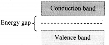
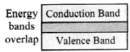
iii. In metals, conduction band and valence band overlap. However, in a semiconductor or an insulator, there is gap between the bottom of the conduction band and the top of the valence band. This is called the energy gap or the band gap.
iv. For metals, the valence band and the conduction band overlap and there is no band gap as shown in figure (b). Therefore, electrons can easily gain electrical energy when an external electric field is applied and are easily available for conduction.
v. In case of semiconductors, the band gap is fairly small, of the order of 1 eV or less as shown in figure (c). Hence, with application of external electric field, electrons get excited and occupy energy levels in conduction band. These can take part in conduction easily.
vi. Insulators, on the contrary, have a wide gap between valence band and conduction band of the order of 5 eV (for diamond) as shown in figure (d). Therefore, electrons find it very difficult to gain sufficient energy to occupy energy levels in conduction band.
vii. Thus, an energy band gap plays an important role in classifying solids into conductors, insulators and semiconductors based on band theory of solids.
Question 2.
Distinguish between intrinsic semiconductors and extrinsic semiconductors
Answer:
Question 3.
Explain the importance of the depletion region in a p-n junction diode.
Answer:
i. The region across the p-n junction where there are no charges is called the depletion layer or the depletion region.
ii. During diffusion of charge carriers across the junction, electrons migrate from the n-side to the p-side of the junction. At the same time, holes are transported from p-side to n-side of the junction.
iii. As a result, in the p-type region near the junction there are negatively charged acceptor ions, and in the n-type region near the junction there are positively charged donor ions.
iv. The potential barrier thus developed, prevents continuous flow of charges across the junction. A state of electrostatic equilibrium is thus reached across the junction.
v. Free charge carriers cannot be present in a region where there is a potential barrier. This creates the depletion region.
vi. In absence of depletion region, all the majority charge carriers from n-region (i.e., electron) will get transferred to the p-region and will get combined with the holes present in that region. This will result in the decreased efficiency of p-n junction.
vii. Hence, formation of depletion layer across the junction is important to limit the number of majority carriers crossing the junction.
Question 4.
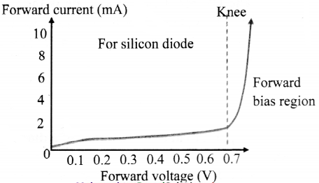
Explain the I-V characteristic of a forward biased junction diode.
Answer:
Question 5.
Discuss the effect of external voltage on the width of depletion region of a p-n junction.
Answer:
11th Physics Digest Chapter 14 Semiconductors Intext Questions and Answers
Internet my friend (Textbookpage no. 256)
i. https://www.electronics-tutorials.ws/diode
ii. https://www.hitachi-hightech.com
iii. https://nptel.ac.in/courses
iv. https://physics.info/semiconductors
v. http://hyperphysics.phy- astr.gsu.edu/hbase/Solids/semcn.html
[Students are expected to visit above mentioned links and collect more information regarding semiconductors.]
Chapter 14 Semiconductors Textbook Exercise Questions and Answers.
1. Choose the correct option.
Question 1.
Electric conduction through a semiconductor is due to:
(A) Electrons
(B) holes
(C) none of these
(D) both electrons and holes
Answer:
(D) both electrons and holes
Question 2.
The energy levels of holes are:
(A) in the valence band
(B) in the conduction band
(C) in the band gap but close to valence band
(D) in the band gap but close to conduction band
Answer:
(C) in the band gap but close to valence band
Question 3.
Current through a reverse biased p-n junction, increases abruptly at:
(A) Breakdown voltage
(B) 0.0 V
(C) 0.3V
(D) 0.7V
Answer:
(A) Breakdown voltage
Question 4.
A reverse biased diode, is equivalent to:
(A) an off switch
(B) an on switch
(C) a low resistance
(D) none of the above
Answer:
(A) an off switch
Question 5.
The potential barrier in p-n diode is due to:
(A) depletion of positive charges near the junction
(B) accumulation of positive charges near the junction
(C) depletion of negative charges near the junction,
(D) accumulation of positive and negative charges near the junction
Answer:
(D) accumulation of positive and negative charges near the junction
2. Answer the following questions.
Question 1.
What is the importance of energy gap in a semiconductor?
Answer:
Question 2.
Which element would you use as an impurity to make germanium an n-type semiconductor?
Answer:
Germanium can be made an n-type semiconductor by doping it with pentavalent impurity, like phosphorus (P), arsenic (As) or antimony (Sb).
Question 3.
What causes a larger current through a p-n junction diode when forward biased?
Answer:
In case of forward bias the width of the depletion region decreases and the p-n junction offers a low resistance path allowing a high current to flow across the junction.
Question 4.
On which factors does the electrical conductivity of a pure semiconductor depend at a given temperature?
Answer:
For pure semiconductor, the number density of free electrons and number density of holes is equal. Thus, at a given temperature, the conductivity of pure semiconductor depends on the number density of charge carriers in the semiconductor.
Question 5.
Why is the conductivity of a n-type semiconductor greater than that of p-type semiconductor even when both of these have same level of doping?
Answer:
3. Answer in detail.
Question 1.
Explain how solids are classified on the basis of band theory of solids.
Answer:
i. The solids can be classified into conductors, insulators and semiconductors depending on the distribution of electron energies in each atom.
ii. As an outcome of the small distances between atoms, the resulting interaction amongst electrons and the Pauli’s exclusion principle, energy bands are formed in the solids.
iii. In metals, conduction band and valence band overlap. However, in a semiconductor or an insulator, there is gap between the bottom of the conduction band and the top of the valence band. This is called the energy gap or the band gap.
iv. For metals, the valence band and the conduction band overlap and there is no band gap as shown in figure (b). Therefore, electrons can easily gain electrical energy when an external electric field is applied and are easily available for conduction.
v. In case of semiconductors, the band gap is fairly small, of the order of 1 eV or less as shown in figure (c). Hence, with application of external electric field, electrons get excited and occupy energy levels in conduction band. These can take part in conduction easily.
vi. Insulators, on the contrary, have a wide gap between valence band and conduction band of the order of 5 eV (for diamond) as shown in figure (d). Therefore, electrons find it very difficult to gain sufficient energy to occupy energy levels in conduction band.
vii. Thus, an energy band gap plays an important role in classifying solids into conductors, insulators and semiconductors based on band theory of solids.
Question 2.
Distinguish between intrinsic semiconductors and extrinsic semiconductors
Answer:
| Intrinsic semiconductors | Extrinsic semiconductors |
| 1. A pure semiconductor is known as intrinsic semiconductors. | The semiconductor, resulting |
| 2. Their conductivity is low | Their conductivity is high even at room temperature. |
| 3. Its electrical conductivity is a function of temperature alone. | Its electrical conductivity depends upon the temperature as well as on the quantity of impurity atoms doped in the structure. |
| 4. The number density of holes (nh) is same as the number density of free electron (ne) (nh = ne). | The number density of free electrons and number density of holes are unequal. |
Explain the importance of the depletion region in a p-n junction diode.
Answer:
i. The region across the p-n junction where there are no charges is called the depletion layer or the depletion region.
ii. During diffusion of charge carriers across the junction, electrons migrate from the n-side to the p-side of the junction. At the same time, holes are transported from p-side to n-side of the junction.
iii. As a result, in the p-type region near the junction there are negatively charged acceptor ions, and in the n-type region near the junction there are positively charged donor ions.
iv. The potential barrier thus developed, prevents continuous flow of charges across the junction. A state of electrostatic equilibrium is thus reached across the junction.
v. Free charge carriers cannot be present in a region where there is a potential barrier. This creates the depletion region.
vi. In absence of depletion region, all the majority charge carriers from n-region (i.e., electron) will get transferred to the p-region and will get combined with the holes present in that region. This will result in the decreased efficiency of p-n junction.
vii. Hence, formation of depletion layer across the junction is important to limit the number of majority carriers crossing the junction.
Question 4.
Explain the I-V characteristic of a forward biased junction diode.
Answer:
Question 5.
Discuss the effect of external voltage on the width of depletion region of a p-n junction.
Answer:
11th Physics Digest Chapter 14 Semiconductors Intext Questions and Answers
Internet my friend (Textbookpage no. 256)
i. https://www.electronics-tutorials.ws/diode
ii. https://www.hitachi-hightech.com
iii. https://nptel.ac.in/courses
iv. https://physics.info/semiconductors
v. http://hyperphysics.phy- astr.gsu.edu/hbase/Solids/semcn.html
[Students are expected to visit above mentioned links and collect more information regarding semiconductors.]